-
Welcome to Zhejiang Mingtehan Electronics Technology Co., Ltd.
13566043962

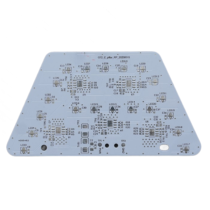
Basic Parameters
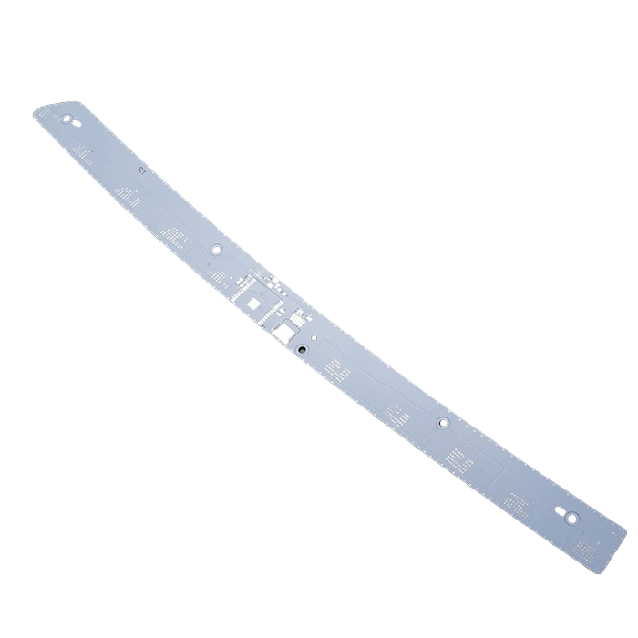
Layers: Double-layer design with two conductive copper layers.
Substrate Material: Typically made from polyimide (PI) or other flexible polymer films.
Board Thickness: Common thicknesses range from 0.2mm to 0.5mm, lightweight and flexible.
Copper Thickness: Generally ranges from 1oz to 2oz.
Minimum Line Width/Spacing: 0.15mm/0.15mm.
Via Type: Plated through holes connect the two layers.
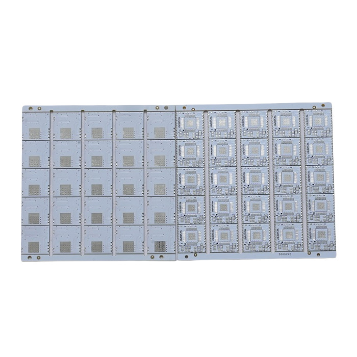
Features
High-Density Routing: Double-layer design allows for more complex wiring layouts, suitable for high-density connections.
Excellent Electrical Performance: Low dielectric constant materials ensure fast signal transmission.
High Flexibility: Capable of bending and folding freely to adapt to complex shapes.
Three-Dimensional Assembly: Supports integration of components and wiring, enabling three-dimensional layout.
Advantages
Design Flexibility: Supports complex circuit designs, suitable for high-density routing.
High Reliability: Reduces wiring errors, enhancing assembly reliability.
Lightweight: Lighter compared to traditional rigid PCBs.
Good Thermal Performance: Efficient heat dissipation helps maintain component performance.
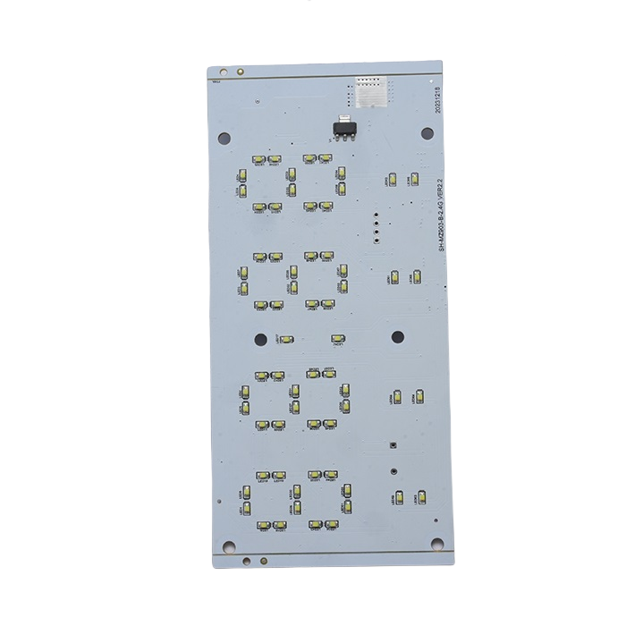
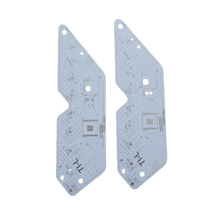
Applications
Consumer Electronics: Such as headphones, smartwatches, and foldable phones.
Wearable Devices: Health monitoring devices, smart clothing.
Automotive Electronics: Sensors and display systems in automotive interiors.
Medical Devices: Portable medical monitoring equipment.
Double-layer flexible PCBs combine high-density routing and excellent electrical performance with the lightweight and high flexibility of flexible boards. They are widely used in consumer electronics, wearable devices, automotive electronics, and medical devices, making them an essential solution in modern electronics manufacturing.