-
Welcome to Zhejiang Mingtehan Electronics Technology Co., Ltd.
13566043962

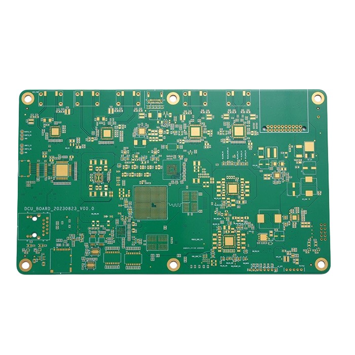
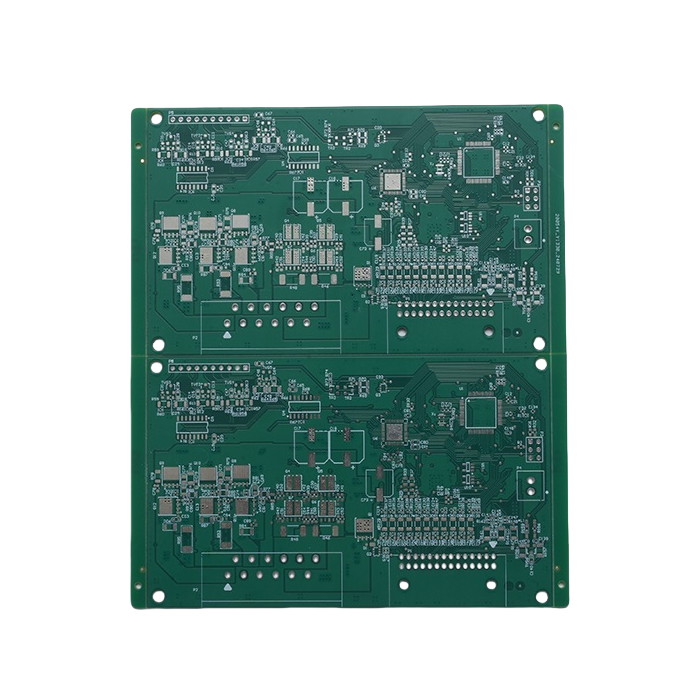
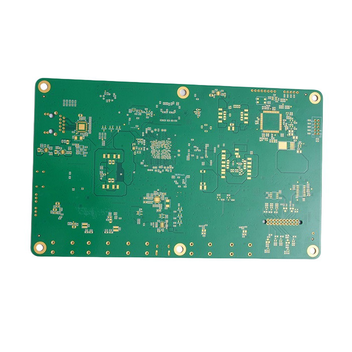
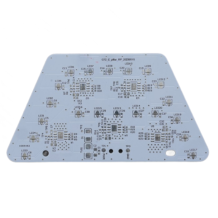
Basic Parameters
Layers: Multi-layer design, typically 3 layers or more, up to 10 layers.
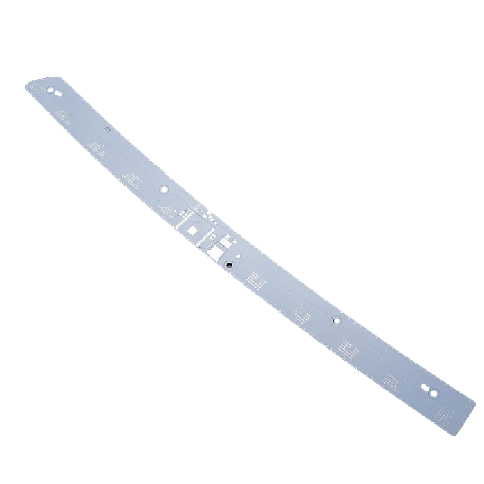
Substrate Material: Typically made from polyimide (PI) or other flexible polymer films.
Board Thickness: Common thicknesses range from 0.2mm to 0.5mm.
Copper Thickness: Generally ranges from 1oz to 3oz.
Minimum Line Width/Spacing: 0.15mm/0.15mm.
Via Type: Plated through holes connect the multiple layers.
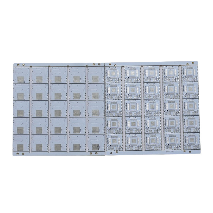
Features
High-Density Routing: Multi-layer design allows for more complex wiring layouts, suitable for high-density connections.
Excellent Electrical Performance: Low dielectric constant materials ensure fast signal transmission.
High Flexibility: Capable of bending and folding freely to adapt to complex shapes.
Three-Dimensional Assembly: Supports integration of components and wiring, enabling three-dimensional layout.
Advantages
Design Flexibility: Supports complex circuit designs, suitable for high-density routing.
High Reliability: Reduces wiring errors, enhancing assembly reliability.
Lightweight: Lighter compared to traditional rigid PCBs.
Good Thermal Performance: Efficient heat dissipation helps maintain component performance.
Durability: Multi-layer structure provides higher durability, suitable for various application environments.
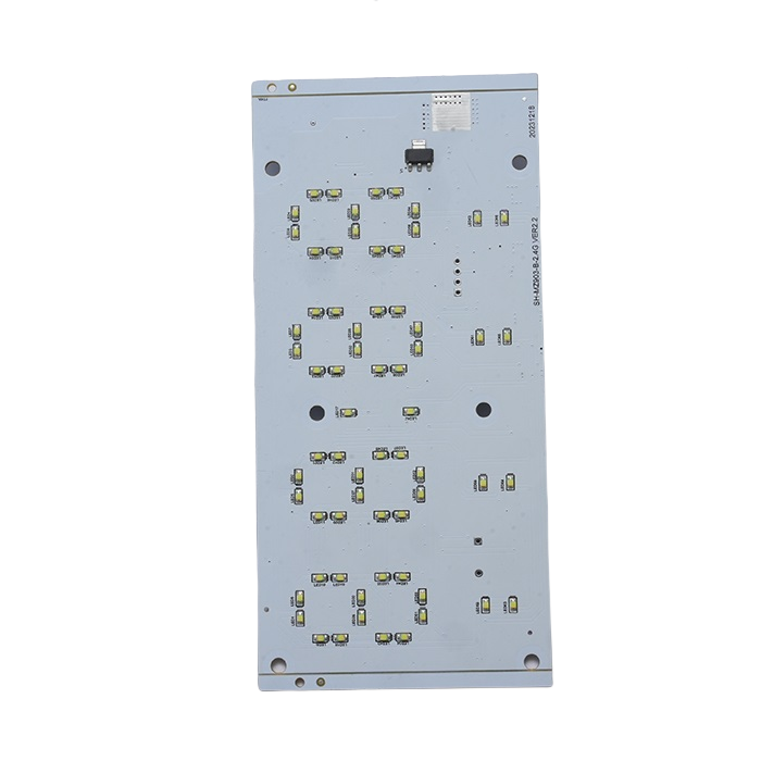
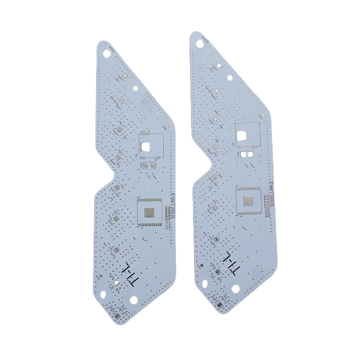
Applications
Consumer Electronics: Such as smartphones, tablets, and headphones.
Wearable Devices: Health monitoring devices, smartwatches.
Automotive Electronics: Sensors and display systems in automotive interiors.
Medical Devices: Portable medical monitoring equipment.
Industrial Applications: Used in robotics and automation equipment, supporting complex wiring.
Multi-layer flexible PCBs are ideal for applications in consumer electronics, wearable devices, automotive electronics, and medical devices due to their high-density routing, excellent electrical performance, and high flexibility. They offer design flexibility and enhance device reliability and durability, making them an essential solution in modern electronics manufacturing.